The Leader in Low NRE,
Low Cost, and Low Volume
Chip Designs
Bay Area Chip Design tackles todays high NRE costs and low volume requirements of cell-based designs
Company Overview
Bay Area Chip Design provides industry-leading ASIC design services and EDA solutions to deliver highly optimized complex ICs in record time. By automating standard cell IC implementation techniques, Bay Area Chip Design delivers quantum improvements in chip-area, performance, power consumption and flexibility.
Company History
Technology Overview
Mid-Volume ASIC design dilemma
Standard Cell ASICs have served our industry well through many process migrations. Now, Moore's law is outstripping the ability to utilize available silicon with an appropriate level of cost and risk. With mask costs passing $1M, design cycles expanding past a year and reliability questions arising from very Deep Sub-Micron physical effects, it now requires a large annual production run to justify a custom device. But, what if you still need the performance of a custom ASIC? Roughly 1/3 of ASIC designs need lower part cost than FPGA (10k-100K volume), but NRE charges, time to market, and total design cost is too high to use cell-based ASIC.
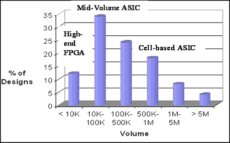
Source: Gartner/Dataquest
The battle for middle ground is best filled by Structured ASICs. Structured ASICs offer a cost-effective solution for the mid-volume market with 75% less development costs than cell-based ASICs and unit costs up-to 90% less than complex FPGAs.
What is Structured ASIC?
Structured ASIC have fewer layers to customize which implies much shorter fabrication time. Structured ASICs have fixed layers to incorporate I/Os, RAMs, Power lines, PLLs, and other IP. Structured ASICs are not Gate Arrays. Gate arrays address the manufacturing cycle time issue with custom ASICs. But, Structured ASICs address the design implementation issues with custom ASICS such as NRE charges, time to handoff, cost of design tools and engineering resources, number of design functions to be performed, IP integration, and unpredictable layout turnaround times of custom ASICs.
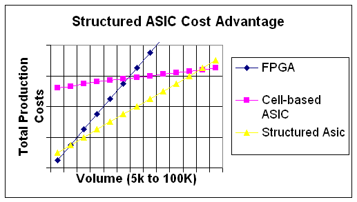
Structured ASIC dramatically shortens the design cycle by simpler design flow which cuts down engineering time by months and reducing fabrication time to weeks compared to months for cell-based ASICs.
Design Services
The Bay Area Chip Design Service Model
In support of the growing trend towards strategic outsourcing and in recognition of high ASIC NRE costs for low and mid volume ASIC designs, Bay Area Chip Design was formed to provide consulting, high-end FPGA conversion, and turn-key ASIC design services. Customers with turnkey approach can provide Bay Area Chip Design with their specification, Verilog/C++ RTL netlist, or gate level Verilog netlist and Bay Area Chip Design delivers timing closure on place and route database to be released to leading foundries.
The Benefits of Outsourcing
To address the issues of mounting design complexity, global competition, resource constraints and time-to-market pressures, more and more semiconductor and system companies are relying upon relationships with external service providers to supply expertise in areas that fall outside of the company’s core competencies and areas of competitive differentiation. These indispensable outsourcing relationships free companies to concentrate their efforts on the areas of greatest value-add, while subsequently allowing the company to benefit from the specialized expertise of external service providers. Such outsourcing arrangements enable companies to introduce new products to the market faster with greater ease.
Capabilities
Bay Area Chip Design has one of the most experienced design teams in the industry, drawing its experience base working with companies like Motorola, LSI Logic, and IBM to name but a few. The Bay Area Chip Design engineering team has many years of experience and each project leader has executed on numbers of high performance designs with a proven track record of delivering complex designs on time. The skill set of the design team is focused in silicon implementation and in achieving the smallest chip area, power consumption optimization and performance maximization. With an eye to quality workmanship and complete customer satisfaction.
Technology
With today’s $1M NREs, the traditional cell-based implementation approach, once the best compromise between time-to-market and cost, is now delivering swollen die sizes at unattractive prices. Bay Area Chip Design offers IC designers a solution to deep sub-micron IC implementation issues while also delivering application specific area optimization. Bay Area Chip Design gives semiconductor design teams the power to create highly optimized chips at dramatically reduced NRE costs within time-to-market schedule demands. The progressive advances in System-on-a-Chip have made semiconductor designs with high numerical calculation content more ubiquitous. Bay Area Chip Design’s technology is especially suited to deal with DSPs, network processors and microprocessors, the important building blocks within today’s SoCs. Bay Area Chip Design provides solutions for deep sub-micron chip designs with feature sizes below 0.18 micron. Performance objectives are achieved with substantially smaller die, lower power, and lower overall cost of silicon. Please refer to Design Services for more information about the Bay Area Chip Design services offered.
Careers
Are you ready to work for the leader in low NRE highly complex chip designs?
Bay Area Chip Design is located in San Jose, California. We invite imaginative and ambitious professionals to join our team as consultants.
Job Listings
Bay Area Chip Design is always on the lookout for top talent. If you're interested in advancing your career with the industry leader in low NRE chip designs, then please check out the current job postings listed below. When submitting your resume, please reference the position desired. Bay Area Chip Design is an equal opportunity employer and offers benefits and compensation packages.
Physical Design Contractor:
-
Responsibilities
- Responsible for all aspects of physical design including timing closure, place and route, clock distribution, IP integration, RC extraction, power and signal integrity analysis, formal verification, DFM, and tapeout.
- Implementation of multimillion gate ASIC designs in the latest technologies.
- Meeting highly challenging schedule, performance, and quality constraints.
- 3+ years of experience in large ASIC physical design implementation on 65 or 90 nanometer technology.
- Experience in Timing closure, place and route and tapeout issues.
- Expertise in Synopsys, Cadence, or Magma physical design tool flow.
- Skill and efficiency in scripting using Tcl or perl desirable.
- Demonstrated ability to work in a team environment.
Qualifications
Management Team
Shahrokh Shakouri – President and Chief Executive Officer
Shahrokh Shakouri founded Bay Area Chip Design as President and CEO in June 2003. Shahrokh has 25+ years experience at various Telecom, Medical, and computer industries specializing on high level behavior modeling and top-down design methodology in ASIC design, synthesis, and simulation. Shahrokh holds an M.S. Electrical Engineering from San Jose State university (May '86) and he has completed Ph. D. courses in EE/CS department at Stanford University (1987-1989).
E-mail: shakouri@BayAreaChipDesign.com
Contact Us
USA Headquarters
Send Message
Where we are
Contact Information
Phone: +1 408 926-4536
Fax: +1 303 845-6648
E-mail: info@BayAreaChipDesign.com